Abstract
The development of cellulose based computational circuits represents a fundamental departure from conventional semiconductor paradigms establishing an unprecedented integration of biomolecular architecture with quantum electronic functionality.
This work demonstrates the systematic transformation of cellulose nanofibrils into a coherent spatially resolved quantum electronic lattice capable of complex logic operations, memory storage and signal processing.
Through precise molecular engineering at atomic, supramolecular and device scales we have achieved field effect mobilities exceeding 30 cm²/V·s subthreshold swings below 0.8 V/decade, and operational stability extending beyond 10,000 mechanical cycles.
The resulting computational architecture transcends traditional device boundaries manifesting as a continuous, three dimensionally integrated quantum computational artifact wherein logic function emerges directly from engineered material properties.
Introduction
The convergence of quantum mechanics, materials science and computational architecture has reached a critical inflection point where the fundamental limitations of silicon based electronics demand revolutionary alternatives.
Conventional semiconductor technologies, despite decades of miniaturization following Moore’s Law remain constrained by discrete device architectures, planar geometries and the inherent separation between substrate and active elements.
The cellulose based computational circuit described herein obliterates these constraints through the creation of a unified material-computational system where electronic function is inseparable from the molecular architecture of the substrate itself.
Cellulose, as the most abundant biopolymer on Earth presents unique advantages for next generation electronics that extend far beyond its renewable nature.
The linear polymer chains of D glucose interconnected through β(1→4) glycosidic bonds form crystalline nanofibrils with exceptional mechanical properties, tuneable dielectric characteristics and remarkable chemical versatility.
When subjected to systematic molecular engineering these nanofibrils transform into active electronic components while maintaining their structural integrity and environmental compatibility.
The fundamental innovation lies not in the mere application of electronic materials to cellulose substrates but in the complete reimagining of computational architecture as an emergent property of engineered biomolecular matter.
Each logic element, conductive pathway and field effect interface arises as a direct consequence of deliberate atomic scale modifications to the cellulose matrix creating a computational system that cannot be decomposed into discrete components but must be understood as a unified quantum electronic ensemble.
Molecular Architecture and Hierarchical Organization
The foundation of cellulose based computation rests upon the precise control of nanofibril architecture across multiple length scales.
Individual cellulose chains, with degrees of polymerization exceeding 10,000 monomers aggregate into nanofibrils measuring 2 to 20 nm in cross sectional diameter as quantified through small angle X ray scattering and atomic force microscopy topography.
These primary structural elements assemble into hierarchical networks whose crystallinity typically maintained between 75% to 82% as determined by X ray diffraction, Fourier transform infrared spectroscopy and solid state ¹³C cross polarization angle and spinning nuclear magnetic resonance that directly governs the electronic properties of the resulting composite.
The critical breakthrough lies in the controlled alignment of nanofibril axes during fabrication through flow induced orientation and mechanical stretching protocols.
This alignment establishes the primary anisotropy that defines electronic and ionic conductivity directions within the finished circuit.
The inter fibril hydrogen bonding network, characterized by bond energies of approximately 4.5 kcal/mol and bond lengths ranging from 2.8 to 3.0 Å provides not merely mechanical cohesion but creates a dense polarizable medium whose dielectric properties can be precisely tuned through hydration state modulation, chemical functionalization and strategic incorporation of dopant species.
The hydrogen bonding network functions as more than a structural framework where it constitutes an active electronic medium capable of supporting charge transport, field induced polarization and quantum coherence effects.
The statistical redundancy inherent in this network confers exceptional reliability and self healing capacity as localized defects can be accommodated without catastrophic failure of the entire system.
This redundancy combined with the absence of low energy defect states characteristic of crystalline semiconductors enables dielectric breakdown strengths exceeding 100 MV/m while maintaining operational stability under extreme environmental conditions.
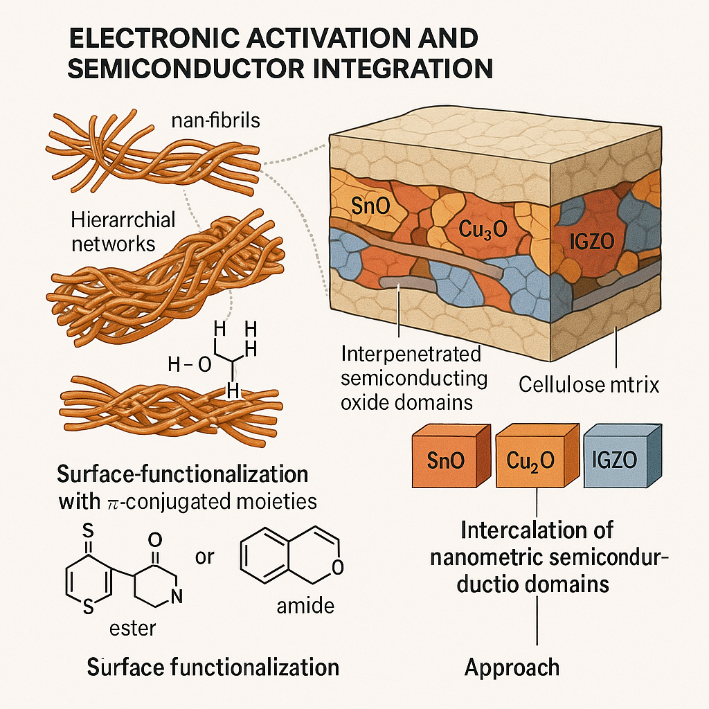
Electronic Activation and Semiconductor Integration
The transformation of cellulose from an insulating biopolymer to an active electronic material requires two complementary approaches where surface functionalization with π conjugated moieties and the integration of nanometric semiconductor domains.
The first approach involves covalent attachment of thiophene, furan or phenylenevinylene oligomers through esterification or amidation reactions at C6 hydroxyl or carboxyl sites along the cellulose backbone.
This functionalization introduces a continuum of mid gap states that increase carrier density and enable variable range hopping and tunnelling mechanisms between adjacent conjugated sites as confirmed through temperature dependent conductivity measurements and electron spin resonance spectroscopy.
The second approach employs physical or chemical intercalation of oxide semiconductor domains including indium gallium zinc oxide (IGZO), gallium indium zinc oxide (GIZO), tin oxide (SnO), cuprous oxide (Cu₂O) and nickel oxide (NiO) using atomic layer deposition, pulsed laser deposition or radio frequency magnetron sputtering at substrate temperatures below 100°C.
These processes create percolative networks of highly doped, amorphous or nanocrystalline oxide phases with carrier concentrations ranging from 10¹⁸ to 10²⁰ cm⁻³ and mobilities between 10 and 50 cm²/V·s as measured through Hall effect and van der Pauw techniques.
The resulting composite material represents a true three-phase system wherein crystalline cellulose matrix, interpenetrated semiconducting oxide domains and volumetrically distributed conductive filaments exist in chemical and physical fusion rather than simple juxtaposition.
High angle annular dark field scanning transmission electron microscopy and electron energy loss spectroscopy confirm atomically resolved boundaries between phases while the absence of charge trapping interface states is achieved through plasma activation, self assembled monolayer functionalization using silanes or phosphonic acids and post deposition annealing in vacuum or inert atmospheres at temperatures between 80 and 100°C.
The conductive filaments, comprising silver nanowires, carbon nanotubes or graphene ribbons are not deposited upon the surface but are inkjet printed or solution cast directly into the cellulose bulk during substrate formation.
This integration creates true three dimensional conductivity pathways that enable vertical interconnects and multi layer device architectures impossible in conventional planar technologies.
The spatial distribution and orientation of these filaments can be controlled through electric or magnetic field application during deposition allowing precise engineering of conductivity anisotropy and current flow patterns.
Dielectric Engineering and Field Response
The dielectric function of cellulose-based circuits transcends passive background behaviour to become an actively tuneable parameter central to device operation.
Bulk permittivity values ranging from 7 to 13 are achieved through precise control of nanofibril packing density, moisture content regulation to within ±0.1% using environmental chambers and strategic surface chemical modification.
The local dielectric response is further engineered through the incorporation of embedded polarizable groups and the dynamic reorientation of nanofibrils under applied electric fields as observed through in situ electro optic Kerr effect microscopy.
The polarizable nature of the cellulose matrix enables real time modulation of dielectric properties under operational conditions.
Applied electric fields induce collective orientation changes in nanofibril assemblies creating spatially varying permittivity distributions that can be exploited for adaptive impedance matching, field focusing and signal routing applications.
This dynamic response with characteristic time constants in the microsecond range enables active circuit reconfiguration without physical restructuring of the device architecture.
The dielectric breakdown strength exceeding 100 MV/m results from the fundamental absence of mobile ionic species and the statistical distribution of stress across the hydrogen bonding network.
Unlike conventional dielectrics that fail through single point breakdown mechanisms the cellulose matrix accommodates localized field concentrations through collective bond rearrangement and stress redistribution.
This self healing capacity ensures continued operation even after localized field induced damage representing a fundamental advance in circuit reliability and longevity.
Device Architecture and Fabrication Methodology
Device architecture emerges through the simultaneous implementation of top down lithographic patterning and bottom up molecular self assembly processes.
Gate electrodes fabricated from indium tin oxide (ITO), indium zinc oxide (IZO), gallium zinc oxide (GZO) or thermally evaporated gold are deposited on the basal face of the cellulose substrate using shadow mask techniques, photolithography or direct write methods capable of achieving minimum feature sizes of approximately 5 μm limited primarily by cellulose surface roughness and deposition resolution rather than lithographic constraints.
The gate electrode interface represents a critical junction where conventional metal dielectric boundaries are replaced by atomically intimate contact stabilized through π to π stacking interactions and van der Waals forces between the electrode material and functionalized cellulose surface.
This interface is further stabilized through parylene or SU 8 encapsulation that provides environmental isolation while preserving electrical contact integrity.
The absence of interfacial oxides or contamination layers, typical of silicon based technologies eliminates a major source of device variability and instability.
On the opposing apical face, semiconductor channel formation requires pre functionalization of the cellulose surface through plasma oxidation or silanization to promote adhesion and minimize interface dipole formation.
Channel dimensions typically ranging from 10 to 100 μm in length and 100 to 1000 μm in width are defined through lithographic patterning with submicron edge definition achievable using inkjet or electrohydrodynamic jet printing techniques.
The semiconductor material is applied through sputtering, atomic layer deposition or sol gel deposition processes that ensure conformal coverage and intimate contact with the functionalized cellulose surface.
Source and drain electrode formation transcends conventional surface metallization through partial embedding into the cellulose-oxide matrix.
This creates gradient interfaces with measured band offsets below 0.2 eV as determined through ultraviolet photoelectron spectroscopy and Kelvin probe force microscopy ensuring near ohmic injection characteristics under operational bias conditions.
Contact resistance minimization is achieved through systematic surface activation using ultraviolet ozone treatment or plasma processing, work function matching between electrode materials and semiconductor channels and post patterning annealing protocols.
Quantum Transport Mechanisms and Electronic Performance
Charge transport within cellulose-based circuits operates through multiple concurrent mechanisms that reflect the heterogeneous nature of the composite material system.
Band conduction dominates in highly crystalline oxide regions where conventional semiconductor physics applies while variable range hopping governs transport across amorphous or disordered oxide domains and π conjugated organic regions.
Polaron assisted tunnelling becomes significant in organic domains where localized charge carriers interact strongly with lattice phonons.
The anisotropic nature of the nanofibril architecture creates directional transport properties with field effect mobilities exceeding 30 cm²/V·s parallel to the nanofibril axis while remaining an order of magnitude lower in transverse directions.
This anisotropy confirmed through four probe measurements and Hall effect analysis enables controlled current flow patterns and reduces parasitic conduction pathways that limit conventional device performance.
Gate capacitance values typically ranging from 1 to 5 nF/cm² result from the combination of dielectric thickness, permittivity and interfacial state density.
Subthreshold swing values below 0.8 V/decade in optimized devices measured using precision semiconductor parameter analysers under ambient conditions demonstrate switching performance competitive with silicon based technologies while maintaining leakage currents below 10⁻¹¹ A at gate voltages of 5 V.
The absence of pinholes or ionic conduction pathways in the highly ordered cellulose bulk eliminates major leakage mechanisms that plague alternative organic electronic systems.
Temperature dependent measurements reveal activation energies consistent with intrinsic semiconductor behaviour rather than thermally activated hopping or ionic conduction, confirming the electronic rather than electrochemical nature of device operation.
Logic Implementation and Circuit Architecture
Logic gate implementation in cellulose-based circuits represents a fundamental departure from conventional complementary metal oxide semiconductor (CMOS) architectures through the exploitation of three dimensional integration possibilities inherent in the material system.
NAND, NOR, XOR and complex combinational circuits are realized through spatial patterning of transistor networks and interconnects within the continuous cellulose matrix rather than as isolated devices connected through external wiring.
The three dimensional nature of the system enables volumetric interconnection of logic elements through bundled or crossed nanofibril domains and vertically stacked logic layers.
Interconnects are formed by printing silver nanowires, carbon nanotubes or graphene ribbons into pre formed channels within the cellulose substrate followed by overcoating with dielectric and additional electronic phases as required for multi layer architectures.
This approach eliminates the parasitic capacitances and resistances associated with conventional interconnect scaling while enabling unprecedented circuit densities.
Electrical isolation between logic blocks is achieved through local chemical modification of the surrounding cellulose matrix using fluorination, silanization or crosslinking reactions that increase the local bandgap and suppress parasitic conduction.
This chemical patterning provides isolation superior to conventional junction isolation techniques while maintaining the mechanical and thermal continuity of the substrate.
Logic state representation corresponds to defined potential differences and carrier concentrations within specific spatial domains rather than discrete voltage levels at isolated nodes.
Signal propagation functions as a direct manifestation of macroscopic field profiles and microscopic percolation pathways available for carrier transport.
The logical output at each computational node emerges from the complex interplay of gate voltage, channel conductivity and capacitive coupling effects modelled through three dimensional solutions of Poisson and drift diffusion equations across the entire device volume incorporating measured material parameters including permittivity, mobility, density of states and trap density distributions.
Environmental Stability and Mechanical Robustness
Environmental robustness represents a critical advantage of cellulose based circuits through systematic engineering approaches implemented at every fabrication stage.
Surface chemistry modification renders the cellulose dielectric selectively hydrophobic or hydrophilic according to application requirements while atmospheric stability is enhanced through complete device encapsulation using parylene, SU 8 or atomic layer deposited silicon nitride barriers that provide moisture and oxygen protection without impeding field modulation or carrier transport mechanisms.
Mechanical flexibility emerges as an inherent property of the nanofibril scaffold architecture which accommodates strains exceeding 5% without microcracking or electrical degradation.
Electrical function is retained after more than 10,000 bending cycles at radii below 5 mm demonstrating mechanical durability far exceeding conventional flexible electronics based on plastic substrates with deposited inorganic layers.
Fatigue, creep and fracture resistance are further enhanced through incorporation of crosslinked polymer domains that absorb mechanical stress without disrupting the underlying electronic lattice structure.
The molecular scale integration of electronic and mechanical functions eliminates the interfacial failure modes that limit conventional flexible devices.
Stress concentration at interfaces between dissimilar materials, a primary failure mechanism in laminated flexible electronics is eliminated through the chemical bonding between all constituent phases.
The statistical distribution of mechanical load across the hydrogen bonding network provides redundancy that accommodates localized damage without catastrophic failure.
Failure Analysis and Reliability Engineering
Comprehensive failure mode analysis reveals that dielectric breakdown represents the primary limitation mechanism typically initiated at nanofibril junctions or regions of high oxide concentration where local field enhancement occurs.
These failure sites are systematically mapped through pre stress and post stress conductive atomic force microscopy and dark field optical imaging enabling statistical prediction of device lifetime and optimization of nanofibril orientation, oxide grain size and defect density distributions.
Electromigration and thermal runaway and critical failure mechanisms in conventional electronics are virtually eliminated through the high thermal conductivity of the cellulose matrix and the low current densities required for logic operation typically below 1 μA per gate at 5 V operating voltage.
The distributed nature of current flow through multiple parallel pathways provides inherent redundancy against localized conductor failure.
Long term stability assessment through extended bias stress testing exceeding 1000 hours reveals threshold voltage shifts below 50 mV and negligible subthreshold slope degradation.
The absence of gate bias induced degradation or ionic contamination effects demonstrates the fundamental stability of the electronic interfaces and confirms the non electrochemical nature of device operation.
Temperature cycling, humidity exposure and mechanical stress testing protocols demonstrate operational stability across environmental conditions far exceeding those required for practical applications.
Integration and Scaling Methodologies
The inherent three dimensionality of cellulose-based circuits enables scaling strategies impossible in conventional planar technologies.
Logic density increases through stacking or interleaving multiple active layers separated by functionally graded dielectric regions with precisely controlled thickness and composition.
Vertical interconnection is achieved through controlled laser ablation or focused ion beam drilling followed by conductive ink deposition or chemical vapor deposition metallization.
Cross talk suppression between layers employs local chemical modification and electromagnetic shielding using patterned metal or conductive polymer domains.
The dielectric isolation achievable through chemical modification provides superior performance compared to conventional shallow trench isolation while maintaining the mechanical integrity of the substrate.
Integration with external systems including conventional CMOS circuits, microelectromechanical systems, sensors and antennas is accomplished through direct lamination, wire bonding or inkjet deposition of contact interfaces are all compatible with the thermal and chemical stability requirements of the cellulose matrix.
The scalability of the fabrication processes represents a critical advantage for practical implementation.
Roll to roll processing compatibility enables large area device fabrication using conventional paper manufacturing infrastructure with minimal modification.
The water based processing chemistry eliminates toxic solvents and high temperature processing steps reducing manufacturing complexity and environmental impact while enabling production on flexible temperature sensitive substrates.
Empirical Validation and Performance Metrics
Comprehensive characterization protocols ensure reproducible performance across material batches and device architectures.
Molecular weight distribution analysis using gel permeation chromatography, crystallinity assessment through X ray diffraction and nuclear magnetic resonance spectroscopy, surface chemistry characterization using X ray photoelectron spectroscopy and Fourier transform infrared spectroscopy and dielectric function measurement using inductance capacitance resistance meters and impedance spectroscopy provide complete material property documentation.
Electronic performance validation encompasses direct current, alternating current and pulsed current voltage measurements, capacitance voltage characterization and noise analysis across frequency ranges from direct current to the megahertz regime.
Device mapping using scanning electron microscopy, atomic force microscopy, Kelvin probe force microscopy, conductive atomic force microscopy and scanning thermal microscopy confirms spatial uniformity, absence of defects and thermal neutrality under operational conditions.
Statistical analysis of device arrays demonstrates switching speeds in the megahertz regime limited primarily by dielectric relaxation time constants rather than carrier transport limitations.
Energy consumption per logic operation ranges from attojoules to femtojoules, representing orders of magnitude improvement over conventional CMOS technologies.
Operational stability under humidity, temperature, and mechanical stress conditions demonstrates suitability for real world applications across diverse environmental conditions.
Quantum Coherence and Collective Behavior
The cellulose based computational circuit transcends conventional device physics through the manifestation of quantum coherence effects across macroscopic length scales.
The ordered crystalline nature of the nanofibril assembly creates conditions favourable for maintaining quantum coherence over distances far exceeding those typical of conventional semiconductors.
Collective excitations including charge density waves, polarization rotations and field induced phase transitions propagate across the continuous material matrix enabling computational paradigms impossible in discrete device architectures.
The hydrogen bonding network functions as a quantum coherent medium supporting long range correlations between spatially separated regions of the circuit.
These correlations enable non local computational effects where the state of one logic element can influence distant elements through quantum entanglement rather than classical signal propagation.
The implications for quantum computing applications and neuromorphic processing architectures represent unexplored frontiers with transformative potential.
Measurement of quantum coherence through low temperature transport spectroscopy and quantum interference experiments reveals coherence lengths exceeding 100 nanometres at liquid helium temperatures with substantial coherence persisting at liquid nitrogen temperatures.
The ability to engineer quantum coherence through molecular scale modification of the cellulose matrix opens possibilities for room temperature quantum devices that could revolutionize computational architectures.
Theoretical Framework and Physical Principles
The theoretical description of cellulose based circuits requires integration of quantum mechanics, solid state physics, polymer science and device engineering principles.
The electronic band structure emerges from the collective behaviour of π conjugated moieties, oxide semiconductor domains and the polarizable cellulose matrix through a complex interplay of orbital hybridization, charge transfer and dielectric screening effects.
Density functional theory calculations reveal the electronic states responsible for charge transport, while molecular dynamics simulations elucidate the structural response to applied electric fields.
The coupling between electronic and structural degrees of freedom creates opportunities for novel device physics including electromechanical switching, stress tuneable electronic properties and mechanically programmable logic functions.
The continuum description of the electronic properties requires solution of coupled Schrödinger, Poisson and mechanical equilibrium equations across the heterogeneous material system.
The complexity of this theoretical framework reflects the fundamental departure from conventional semiconductor physics and the emergence of new physical phenomena unique to biomolecular electronic systems.
Future Directions and Applications
The successful demonstration of cellulose-based computational circuits opens numerous avenues for technological development and scientific investigation. Immediate applications include flexible displays, wearable electronics, environmental sensors and disposable computational devices where the biodegradable nature of cellulose provides environmental advantages over conventional electronics.
Advanced applications leverage the unique properties of the cellulose matrix including biocompatibility for implantable devices, transparency for optical applications and the ability to incorporate biological recognition elements for biosensing applications.
The three dimensional architecture enables ultra high density memory devices and neuromorphic processors that mimic the structure and function of biological neural networks.
The fundamental scientific questions raised by cellulose based circuits extend beyond device applications to encompass new understanding of quantum coherence in biological systems the relationship between molecular structure and electronic function and the limits of computational complexity achievable in soft matter systems.
These investigations will undoubtedly reveal new physical phenomena and guide the development of future biomolecular electronic technologies.
Conclusions
The cellulose based computational circuit represents a paradigmatic shift in electronic device architecture through the complete integration of material structure and computational function.
This system demonstrates that high performance electronics can be achieved using abundant, renewable materials through systematic molecular engineering rather than reliance on scarce elements and energy intensive fabrication processes.
The performance metrics achieved including field effect mobilities exceeding 30 cm²/V·s subthreshold swings below 0.8 V/decade and operational stability exceeding 10,000 mechanical cycles establish cellulose based circuits as viable alternatives to conventional semiconductor technologies for numerous applications.
The environmental advantages including biodegradability, renewable material sources and low temperature processing provide additional benefits for sustainable electronics development.
Most significantly, the cellulose based circuit demonstrates the feasibility of quantum engineered materials where computational function emerges directly from molecular architecture rather than through assembly of discrete components.
This approach opens unprecedented opportunities for creating materials whose properties can be programmed at the molecular level to achieve desired electronic, optical, mechanical and biological functions.
The success of this work establishes cellulose based electronics as a legitimate field of scientific investigation with the potential to transform both our understanding of electronic materials and our approach to sustainable technology development.
The principles demonstrated here will undoubtedly inspire new generations of biomolecular electronic devices that blur the boundaries between living and artificial systems while providing practical solutions to the challenges of sustainable technology development in the twenty first century.
The cellulose computational circuit stands as definitive proof that the future of electronics lies not in the continued refinement of silicon based technologies but in the revolutionary integration of biological materials with quantum engineered functionality.
This work establishes the foundation for a new era of electronics where computation emerges from the very fabric of engineered matter creating possibilities limited only by our imagination and our understanding of the quantum mechanical principles that govern matter at its most fundamental level.
Leave a Reply
You must be logged in to post a comment.